Precision Cutting × Smart Inspection
One-Stop PCB Automation Integration Solutions
Syn Dyna Technology specializes in automated inspection equipment, precision cutting measurement, and advanced optical vision recognition systems, helping the semiconductor and PCB industries comprehensively improve process yield.
About Syn Dyna
Founded in December 2009, Syn Dyna Technology has a complete R&D team integrating mechanical automation design control with vision detection systems.
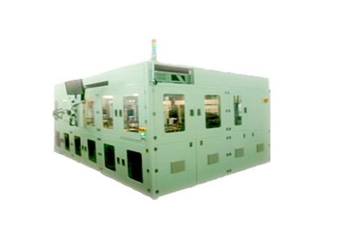
ACMD-2000 IN-Line Post-Cutting Dimension Inspection Machine
View details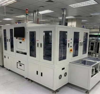
ACMD-2000 IN-Line Post-Cutting Dimension Inspection Machine
View details- 1. Control System: High-precision servo control on each axis, integrated with user-friendly software for easy operation
- 2. Conveying Mechanism: High-precision servo control with dedicated carriers for infeed; TRAY transfer for OK output
- 3. Pick-and-Place Arm: Independently actuated vacuum nozzles pick up boards, sorting OK, NG, and X boards separately
- 4. Optical Inspection: Non-contact optical imaging with vision software for custom region selection
- 5. Data Upload: Reads 2D barcodes on each board during inspection with real-time measurement data upload
- 6. Optional board height measurement function
Auto Laser Marking Machine
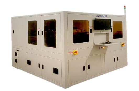
Auto Laser Marking Machine
- 1. Laser sample marking with pre-process defect import; integrates manual defect marking detection, completing both sides in a single pass without repositioning.
- 2. Equipment size: W2000mm * D2000mm * H1900mm.
- 3. Key functions: Integrates front-end AOI, ET, and AVI with manual marking data to perform PCB substrate marking, gold blackening, solder mask whitening, 2D code and plain code printing.
- 4. High-resolution line-scan CCD paired with a 1um optical scale for high-precision printing standards.
- 5. Dual X-Y stages with the industry's largest table size of L290*W150mm, accommodating substrate sizes L:85~290mm; W:40~150mm, covering over 95% of substrate part numbers.
MP Thermoforming Machine
MP Thermoforming Machine
- 1. Equipment size: W3000mm*D2000mm*H2050mm.
- 2. MP IC substrate size 300x300mm; supports board thickness 0.6~2mm (based on MP tray dimensions).
- 3. Up to 60 pieces loaded at once, produced automatically via 3 independent infeed/outfeed systems and heating platforms, operable simultaneously or individually.
- 4. Real-time feedback precision control of heating platform temperature, with fluctuation within +/- 2%.
- 5. Heating platform vacuum suction up to -85kpa, with automatic compensation and variation within +/- 2 kpa.
- 6. Equipped with positioning CCD to check infeed direction and position before loading, preventing errors.
- 7. Nitrogen is injected into the sealed oven chamber during production, with precise flow control and gas concentration detection.
- 8. Interface displays real-time heating temperature, time, vacuum suction, pressure, flow rate, and uploads production data
Why Choose Us?
We are dedicated to automation technology, combining machine vision production equipment to provide the electronics industry with sound operational methods and structural potential.
Quality
Improves customer post-process yield by 10-20% in real deployments.
Service
We help customers boost profitability with strong flexibility in the shortest time, strengthening their competitive edge.
Professional
Innovative design and diverse products spanning semiconductors, PCB, FPD, and LED.
28
Clients Served
48
R&D Projects
56,868
Service Hours
17
Years of Growth
Core Technology & Equipment
Comprehensive optical inspection, laser processing, and custom automation integration services
Substrate Laser Marking
High-precision laser marking technology for various substrates, ensuring clear barcodes and text for wafer and chip traceability.
Layer Offset Inspection
Precise layer offset measurement for high-density multilayer boards (HDI), ensuring process yield.
Our Clients